Share with others:
A revolution in home PCB manufacturing!
Today’s professional printed circuit board (PCB) manufacturing services offer exceptional quality at affordable prices. They can often be completed in as little as a week. But when you need to test and change designs quickly, waiting isn’t always an option. That’s where home-made PCB manufacturing methods come in. However, they have one big problem: the transitions between layers, called “vias.”
Vias are like copper tunnels that connect conductors between different layers of a PCB. Without them, it is often impossible to route a conductor without crossing another. But making vias at home is challenging - traditional methods such as etching, milling and laser engraving do not make it easy.
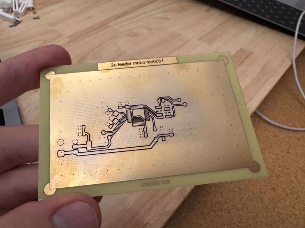
Stephen Hawes presented a solution that the community has dubbed “Biscuit Board” (the project is called Viagrid on GitHub). It is a blank PCB board with pre-placed vias in standard locations. The PCB designer downloads a template with the via locations and uses them to design the leads. Then, using a laser or CNC router, they cut the leads and the vias are already where they need to be.
Another important element of the Biscuit Board is the precise positioning of the origin. Hawes designed the board with UV laser engravers like the ComMarker Omni 1 and Omni X in mind. The corners of the board have special shapes that allow the laser preview to be precisely aligned with the vias. CNC milling users can set the origin even more precisely using traditional methods.
This is one of those ideas that is simply useful. If you have a stock of Biscuit Boards, you are ready to quickly prototype PCBs with vias. If the idea takes hold, we can easily imagine Biscuit Boards in different shapes, sizes, and via densities.